Transistor symbols
Pieter-Tjerk de Boer, PA3FWM web@pa3fwm.nl(This is an adapted version of part of an article I wrote for the Dutch amateur radio magazine Electron, September 2023.)
On June 30, 2023, it was 75 years ago that Bell Labs (the research institute of the American telephone company) announced their invention of the transistor. However, that first transistor was not the well-known NPN or PNP junction transistor that went on to change the world, but the so-called 'point-contact transistor'. It works differently and soon went into oblivion, but its structure lives on in the symbol used in schematics for the junction transistor.
Junction and point-contact transistors
Transistors consist of a piece of very pure semiconductor material (back then germanium, nowadays silicon). In it, some contaminations have been carefully applied which make the material conductive: N-type material has free electrons, while P-type material has free electron-less spots, called 'holes', which can move through the material as if they were positive charges.
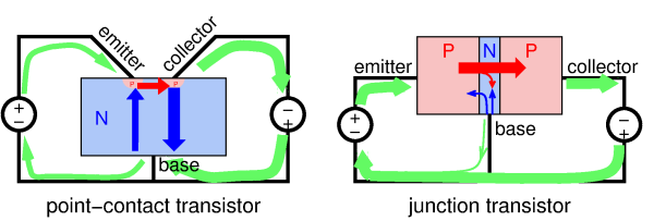 In this figure (based on [1]) we compare the structure and working principles of both types of transistor.
The arrows indicate the currents: green shows the current in the wires, red the flow of 'holes' in
the semiconductor material, and blue the flow of electrons in the semiconductor material.
It may seem as if the blue arrows are the wrong way around, but remember that electrons are
negatively charged, so they move in the opposite direction of how 'the current' flows.
In this figure (based on [1]) we compare the structure and working principles of both types of transistor.
The arrows indicate the currents: green shows the current in the wires, red the flow of 'holes' in
the semiconductor material, and blue the flow of electrons in the semiconductor material.
It may seem as if the blue arrows are the wrong way around, but remember that electrons are
negatively charged, so they move in the opposite direction of how 'the current' flows.
First consider the junction transistor, at the right in the figure. A PNP transistor is characterized by having two P-type regions, with an N-type region in between. Each place where P and N meet is called a 'junction' and is essentially a diode: current can only flow if the P-side is positive w.r.t. the N-side. Viewed this way, the junction transistor consists of two diodes. In normal use, the base-emitter diode is given a voltage in its conducting direction ('forward biased'), while the base-collector diode is reverse biased. Thus a current can flow through the base-emitter junction, but no current should flow through the collector. The 'transistor effect' is that the 'holes' from the P-type emitter material, when they enter the N-type base region, can 'overshoot' into the P-type collector region. Thus, a current will in fact flow through the collector. What's more, the lion's share of the emitter current goes to the collector, as indicated by the thickness of the arrows. The ratio between base and collector currents is the transistor's current amplification factor, indicated by β, which can easily be 100 or more.
Next consider the point-contact transistor, left in the figure. It consists of only a piece of N-type material, in which two point-shaped contacts have been pushed, very close to each other. At each contact, a small P-type region automatically arises, resulting in diode-like operation, like in the junction transistor. But the currents are different. Part of the emitter current goes to the base, as electrons. Another part goes to the collector, as holes; those holes are positively charged and are thus attracted by the collector. There they disturb the reverse-biased diode, resulting in a substantial flow of electrons between the collector and the base. Compared to the junction transistor, the base current is much larger, and in the opposite direction. The relevant current amplification factor of the point-contact transistor is the ratio between the collector and emitter currents, or rather, changes of these currents; this ratio is denoted by α and typically 2 to 3.
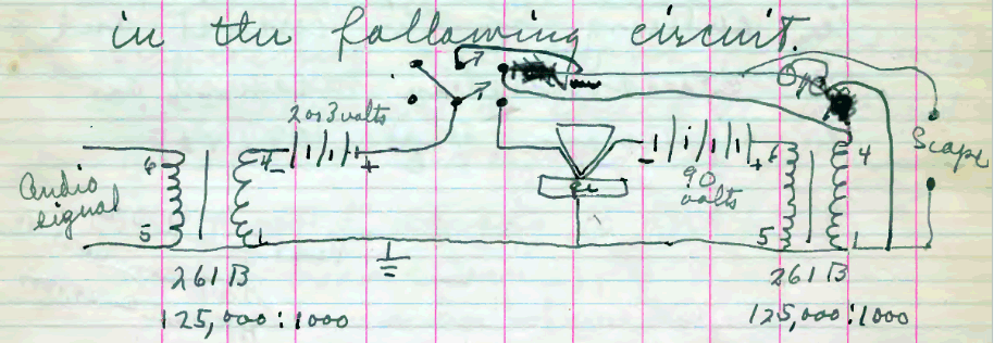 The next figure shows the schematic of the first audio amplifier made with a point-contact transistor,
as shown in Brattain's lab notebook, December 1947 [3].
Note the collector voltage of no less than 90 volts.
Which such a high voltage, the relatively small current amplification factor still allows a decent
power amplification (about 20 dB).
The next figure shows the schematic of the first audio amplifier made with a point-contact transistor,
as shown in Brattain's lab notebook, December 1947 [3].
Note the collector voltage of no less than 90 volts.
Which such a high voltage, the relatively small current amplification factor still allows a decent
power amplification (about 20 dB).
Practical realisation
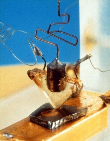 This figure shows the very first point-contact transistor, made in December 1947 at Bell Labs [4].
It consists of a slice of germanium with N-type doping, and a triangular piece of plastic
over which a piece of gold foil has been folded, and cut at the point of the triangle.
That point has subsequently been pushed into the germanium, so the two halves of the gold foil
touch the germanium in close proximity: those are the two point contacts.
This figure shows the very first point-contact transistor, made in December 1947 at Bell Labs [4].
It consists of a slice of germanium with N-type doping, and a triangular piece of plastic
over which a piece of gold foil has been folded, and cut at the point of the triangle.
That point has subsequently been pushed into the germanium, so the two halves of the gold foil
touch the germanium in close proximity: those are the two point contacts.
The junction transistor is much harder to make. It's crucial that the base is very thin. If the base is too thick, the holes coming from the emitter can't reach the collector before getting 'filled' by free electrons from the N-type base material. (For the same reason the emitter and collector contacts in the point-contact transistor must also be close to each other.) And if you've managed to make the two junctions with such a very thin base layer in between, you still have to connect a wire to that base. All of this didn't succeed until 1949 [5].
The simpler structure of the point-contact transistor also meant that amateurs could make them themselves, by taking germanium from a diode and, very carefully, punching two wires into it and mounting them stably [6]. Such a transistor can even be repaired, by punching in the wires anew.
Schematic symbols
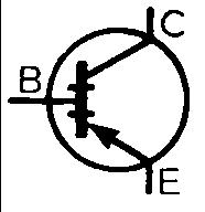
 You've probably noticed the similarity between the well-known schematic symbol for transistors, and
the physical structure of the point-contact transistor shown in the above figures:
a thick line for the base germanium block, and two slanted lines, one with an arrow,
representing the emitter and collector point contacts.
Clearly, this symbol is based on the structure of the point-contact transistor,
but we're still using it for the junction transistor, despite the latter's completely different structure.
You've probably noticed the similarity between the well-known schematic symbol for transistors, and
the physical structure of the point-contact transistor shown in the above figures:
a thick line for the base germanium block, and two slanted lines, one with an arrow,
representing the emitter and collector point contacts.
Clearly, this symbol is based on the structure of the point-contact transistor,
but we're still using it for the junction transistor, despite the latter's completely different structure.
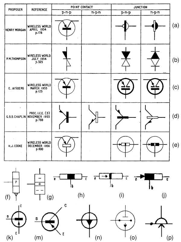
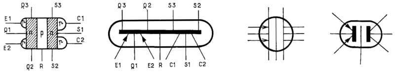
In the 1950s several proposals have been made for a more suitable symbol for the junction transistor. The figure gives an (undoubtedly incomplete) overview, copy-pasted from various publications [7-14]. It may look like a chaotic collection, but we can sort the symbols into several categories.
A first category comprises symbols based on the physical structure. That can be done schematically, like the p-n-p or n-p-n blocks in symbols (e)-(j). Symbol (a) goes even further: it's a sketch of the real structure of alloy junction transistors, namely a thin plate of N-type germanium with a 'drop' of P-type germanium on each side (or P and N reversed for an NPN transistor, of course). Symbol (p) seems inspired by this, but with an arrow instead of a drop as the emitter.
A second category comprises symbols based on the existing point-contact transistor symbol. In proposals (d), (k), (m) and (n), the collector and emiter are shown on opposite sides of the base, which is characteristic for how a junction transistor is structured. On the other hand, (c) keeps them on the same side of the base; by comparison this is a rather odd choice, but the symbol still emphasizes the layered structure, and has been the house style of the French magazien Toute la Radio [9] for many years.
Finally, there are two proposals that emphasize the relationship to other components. Proposal (b), from Canada, emphasizes the PN junctions, by drawing those as diodes. On the other hand, proposal (o) from RCA emphasizes the similarity to the vacuum tube: not in terms of physical structure, but in terms of function.
The only thing most symbols agree on, is the arrow indicating the emitter, and the fact that this arrow points outward for NPN and inward for PNP. Only symbols (a), (b), (g) and (h) don't have an emitter arrow, and in (e) the arrow direction doesn't indicate PNP/NPN.
Conference
Such a variety of schematic symbols is of course unpractical. Therefore, in 1961 an international conference was held to take a decision in this matter [14, 15]. There were two proposals on the table. One boiled down to simply keep using the point-contact transistor symbol also for the junction transistor. The other proposal came from Belgium and France. I'm not completely certain on this, but based on [10] I suspect this proposal was symbol (m) from the previous figure.
 In fact, the discussion was not just about these two symbols themselves, but also about how the
symbols could be extended to future components with more than two junctions.
That's illustrated in the adjacent figure, copied from [10].
This figure shows at the left a hypothetical component with six P-N junctions and no less than eleven wires,
and to the right various (equally hypothetical) schematic symbols for it, according to the various proposals.
With today's knowledge we may laugh at this, but back then it was expected that components
with more P-N junctions were a likely future development.
Indeed, components have been developed with more P and N regions, such as the thyristor (four regions)
and the triac, but that's about where it stopped.
And for those components, new symbols have been designed that do not fit the systematic approach illustrated here.
Nowadays, components are made with very many (even billions) P-N junctions on one piece of sillicon,
but we call those integrated circuits and they consist of lots of separate transistors that can
be represented by the simpler standard symbols.
In fact, the discussion was not just about these two symbols themselves, but also about how the
symbols could be extended to future components with more than two junctions.
That's illustrated in the adjacent figure, copied from [10].
This figure shows at the left a hypothetical component with six P-N junctions and no less than eleven wires,
and to the right various (equally hypothetical) schematic symbols for it, according to the various proposals.
With today's knowledge we may laugh at this, but back then it was expected that components
with more P-N junctions were a likely future development.
Indeed, components have been developed with more P and N regions, such as the thyristor (four regions)
and the triac, but that's about where it stopped.
And for those components, new symbols have been designed that do not fit the systematic approach illustrated here.
Nowadays, components are made with very many (even billions) P-N junctions on one piece of sillicon,
but we call those integrated circuits and they consist of lots of separate transistors that can
be represented by the simpler standard symbols.
At the conference it initially looked like most participants would support the French-Belgian proposal; according to [14] only the Dutch delegation supported the American proposal. But eventually the American proposal was selected by a large majority, and as a consequence we still draw point-contact transistors in our schematics nowadays.
Not everyone was immediately convinced by the conference outcome. I found symbol (n) in a 1966 publication, and IBM kept using their own symbol (h), with some variations, into the 1980s. And one finds the French symbol (m) in some French magazines and books into the 1970s.
The inventors
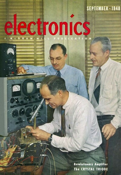 John Bardeen, Walter Brattain and William Shockley are widely considered the inventors of the transistor
(even though in some places other people are given this honour).
They posed for photographers at the occasion of the public announcement of the invention in June 1948.
However, this photo is a bit fishy.
John Bardeen, Walter Brattain and William Shockley are widely considered the inventors of the transistor
(even though in some places other people are given this honour).
They posed for photographers at the occasion of the public announcement of the invention in June 1948.
However, this photo is a bit fishy.
Shockley is sitting prominently at the microscope, while Bardeen and Brattain look on from the background. But the only transistor that can be under the microscope is the point-contact transistor, and that was invented by Bardeen and Brattain, without Shockley! In spite of this, Bell Labs had decided that Shockley should also be in all pictures. Shockley was 'just' the boss of Bardeen and Brattain. As a theoretician, he had worked for years on ideas to amplify signals using semiconductor material, but had not yet come to something that worked. That was achieved by Bardeen (also a theoretician) and Brattain (an experimenter) together.
Shockley couldn't live with that and thought long and hard about the matter in January 1948; purely theoretically he then came up with the junction transistor, which however could not yet be fabricated. Eventually, but this was of course unknown in 1948, that junction transistor would become much more important than the point-contact transistor, even though the latter was invented earlier. So from that point of view it is justified that in 1956 Shockley, together with Bardeen and Brattain, received the Nobel prize.
After his time at Bell Labs, Shockley set up his own company to develop transistors, in what later became known as Silicon Valley. But that wasn't a success; due to his bad management his best employees left, to first found Fairchild Semiconductor, and later Intel. Later in life, Shockley advocated eugenetics and was no longer taken seriously in science.
In that sense, Bardeen was more successful; he got to go to Stockholm in 1972 for another Nobel prize, this time for his work on superconductivity.
If you want to read much more about the invention and the inventors of the transistor, I'd recommend [5]. And if you happen to see yet another junction transistor symbol than the ones in 'my' collection in the above figure, please let me know!
Addendum
Since writing the above, I have encountered a few more symbols.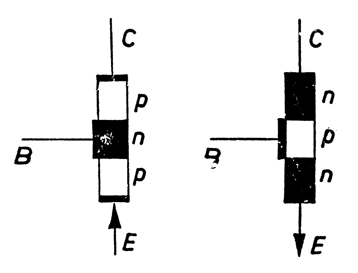
The first pair is from [16]. This booklet uses the 'usual' point-contact-based symbols, but shows this symbol too, with the remark that it is found sporadically (German: 'vereinzelt') in the literature. It's clearly a variation of symbols (e), (h), and (i).
 The next symbol is from a Greek book, [17].
This book shows it in a large table of symbols, together with the normal point-contact symbol
and symbols (c) and (k).
The book doesn't say why it gives four symbols, or even that this symbol is
for the junction transistor, but it might well be:
it's clearly based on the standard point-contact symbol, with two dashes added which
might be taken to indicate the layered structure.
The next symbol is from a Greek book, [17].
This book shows it in a large table of symbols, together with the normal point-contact symbol
and symbols (c) and (k).
The book doesn't say why it gives four symbols, or even that this symbol is
for the junction transistor, but it might well be:
it's clearly based on the standard point-contact symbol, with two dashes added which
might be taken to indicate the layered structure.
 The next few are from an article [18] in Radio Mentor (a German magazine) with various symbols
and their rationale, and some industry comments.
First, the symbol that Radio Mentor themselves are using: the usual one, except that the C and E connections
are not slanted but at right angles to the base.
The next few are from an article [18] in Radio Mentor (a German magazine) with various symbols
and their rationale, and some industry comments.
First, the symbol that Radio Mentor themselves are using: the usual one, except that the C and E connections
are not slanted but at right angles to the base.
 Next a set of variations of the "usual" symbol, with various patterns of lines in the
rectangle to symbolize the depletion layer.
Next a set of variations of the "usual" symbol, with various patterns of lines in the
rectangle to symbolize the depletion layer.
 The left one of these is said to be the proposal of the DIN 40700 standard for the point-contact transistor.
It's not explicit from the text whether that also holds for the right symbol for the junction transistor.
The left one of these is said to be the proposal of the DIN 40700 standard for the point-contact transistor.
It's not explicit from the text whether that also holds for the right symbol for the junction transistor.
The response from the TE-KA-DE company in [18] remarks that they use the "usual" symbol, but always with the arrow pointing to the base. Whether the transistor is PNP or NPN should thus be concluded from the type number or the surrounding circuitry. In a sense, this is not unlogical, with the arrow into the base symbolizing the point contact: someone at some point must have come up with the idea of reversing the arrow for NPN...
 Funkschau spent (at least?) two articles on this topic in 1954 [19], showing various symbols
(most of which we've already seen above) and quoting various people from industry about their
preferences.
Perhaps the most noteworthy is this one, where instead of a new symbol for junction transistors,
new symbols for point-contact transistors are proposed, and matching symbols for point-contact diodes
(to distinguish them from junction diodes).
Funkschau spent (at least?) two articles on this topic in 1954 [19], showing various symbols
(most of which we've already seen above) and quoting various people from industry about their
preferences.
Perhaps the most noteworthy is this one, where instead of a new symbol for junction transistors,
new symbols for point-contact transistors are proposed, and matching symbols for point-contact diodes
(to distinguish them from junction diodes).
Both [18] and [19] discuss the issue of whether or not to draw a circle around the symbol. Some prefer this for clarity (making the transistor stand out just like tubes do), others find it useless (as, in contrast to tubes, there's no vacuum enclosure). One company spokesperson suggests to only draw the circle in case of junction transistors. Of course, the current-day habit of drawing a circle only around discrete transistors but not around those in an IC was not on the horizon yet in those days (1954).
 This very different symbol was proposed by a reader of Electronic Engineering [20],
who wanted to emphasize that there can be a substantial potential difference between
the collector (the wire ending an blob) and the base and emitter.
I checked the next few issues of the magazine, but there seems to have been no follow-up to his suggestion.
This very different symbol was proposed by a reader of Electronic Engineering [20],
who wanted to emphasize that there can be a substantial potential difference between
the collector (the wire ending an blob) and the base and emitter.
I checked the next few issues of the magazine, but there seems to have been no follow-up to his suggestion.
References
[1] https://spectrum.ieee.org/transistor-history[2] William Shockley: Electrons and Holes in Semiconductors, 1950
[3] https://bellsystemmemorial.com/belllabs_transistor.html
[4] https://www.computerhistory.org/revolution/digital-logic/12/273
[5] Michael Riordan en Lillian Hoddeson: Crystal Fire: The Invention of the Transistor and the Birth of the Information Age, 1997
[6] P.B. Helsdon: Home-Made Transistors, Wireless World, Jan. 1954
[7] M. Scroggie (Cathode Ray): Transistor Graphical Symbols, Wireless World, April 1957
[8] Howard E. Tompkins: Foreword to Transistor Papers, IRE Transactions on Circuit Theory, 1957
[9] H. Schreiber: Comment représenter les transistors?, Toute la Radio, Mars-Avril 1955
[10] H. Schreiber: Les symboles graphiques des semiconducteurs, Toute la Radio, Janvier 1962
[11] K.B. Hansen: Logic Circuits with Complementary Transistors, 1966; https://orbit.dtu.dk/en/publications/logic-circuits-with-complementary-transistors
[12] IBM SLT Designer's Handbook, Oct. 1968; http://bitsavers.org/pdf/ibm/logic/
[13] Edward Jones-Imhotep: Icons and Electronics, Historical Studies in the Natural Sciences, 2008
[14] Technically Speaking, IEEE Spectrum, July 1987
[15] Sorab (Soli) K. Ghandhi: Saving the Transistor Symbol; https://ethw.org/First-Hand:Saving_the_Transistor_Symbol
[16] Horst Putzmann: Kristalldioden und Transistoren (Der praktische Funkamateur, Band 3). Not dated, probably around 1960.
[17] Νικ. Μ. Χενου: Ηλεκτρονικο σχεδιο. 1984.
[18] Symbole und Namen in der Transistoren-Technik. Radio Mentor, Juli 1954.
[19] Herbert G. Mende: Wir stellen zur Diskussion: Transistor-Symbole. Funkschau, 1954, Heft 1 and 10.
[20] L. Molyneux: Transistor Symbol. Letters to the editor, Electronic Engineering, April 1954.
Text on this page is copyright 2023, P.T. de Boer, web@pa3fwm.nl .
Republication is only allowed with my explicit permission.